This 2-layer rigid PCB adheres to international industry standards to ensure dependable performance. It adopts F4BTMS615 as its base substrate, which is specifically designed to fulfill the strict requirements of aerospace, microwave, and RF applications, boasting superior electrical, mechanical, and thermal properties.
PCB Specification
| Item | Details |
| Base Material | F4BTMS615 |
| Layer Count | 2 layers |
| Board Dimensions | 45.8mm x 102.1mm, 1 Piece, with a tolerance of +/- 0.15mm |
| Minimum Trace/Space | 4/5 mils |
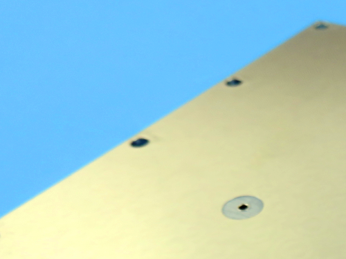
| Minimum Hole Size | 0.3mm |
| Finished Board Thickness | 0.3mm |
| Finished Copper Weight | 1 oz (1.4 mils) for outer layers |
| Via Plating Thickness | 20 μm |
| Surface Finish | Immersion Tin |
| Silkscreen | No silkscreen is applied to either the top or bottom layer |
| Solder Mask | No solder mask is applied to either the top or bottom layer |
| Quality Control | A 100% electrical test is performed before shipment |
PCB Stack-up
The 2-layer rigid PCB is designed with an optimized stackup structure, which is customized to enhance mechanical stability, electrical performance, and thermal conductivity. The layers from top to bottom are as follows:
| Layer | Specifications |
| Copper Layer 1 | 35 μm |
| F4BTMS615 Core | 0.254 mm (10 mil) |
| Copper Layer 2 | 35 μm |
Artwork and Quality Standard
Artwork Format Supplied: Gerber RS-274-X, the global industry standard for PCB manufacturing, ensuring compatibility with mainstream equipment and software for accurate design data transmission and reduced deviations.
Quality Standard: IPC-Class-2, a widely accepted benchmark with strict requirements for material, dimension, electrical and mechanical performance to meet high-performance electronic applications with moderate reliability.
Availability
This PCB is offered for global shipping, with support for international logistics to cater to the varied needs of overseas projects and guarantee prompt delivery.
Introduction to F4BTMS Base Material
The F4BTMS series is an upgraded iteration of the F4BTM series, with technological advancements in material formulation and manufacturing techniques. By adding a substantial quantity of ceramics and reinforcing with ultra-thin, ultra-fine glass fiber cloth, the material’s performance has been significantly enhanced, and it offers a wider range of dielectric constants. It is a high-reliability material suitable for aerospace use and can serve as a substitute for similar foreign products.
Through the integration of a small amount of ultra-thin, ultra-fine glass fiber cloth and a large quantity of uniformly dispersed special nano-ceramics mixed with polytetrafluoroethylene resin, the material reduces the adverse impact of glass fiber on electromagnetic wave propagation. This leads to lower dielectric loss, improved dimensional stability, reduced X/Y/Z anisotropy, an expanded usable frequency range, enhanced electrical strength, and increased thermal conductivity. Furthermore, it possesses an excellent low coefficient of thermal expansion and stable dielectric temperature characteristics. The F4BTMS series is equipped with RTF low-roughness copper foil as standard, which lowers conductor loss and ensures excellent peel strength, and it is compatible with both copper and aluminum substrates.
Key Features of F4BTMS615 Material
| Key Features | Specifications & Descriptions |
| Dielectric Constant (Dk) | 6.15 at 10GHz |
| Dissipation Factor | 0.0020 at 10GHz; 0.0023 at 20GHz |
| Coefficient of Thermal Expansion (CTE) | X-axis: 10 ppm/°C; Y-axis: 12 ppm/°C; Z-axis: 40 ppm/°C (-55°C to 288°C) |
| Thermal Coefficient of Dk | -96 ppm/°C (-55°C to 150°C) |
| Thermal Conductivity | 0.67 W/mk |
| Moisture Absorption | 0.1% |
Typical Applications
-Aerospace equipment, space and cabin equipment
-Microwave and RF devices
-Radar, military radar
-Feed networks
-Phase-sensitive antennas, phased array antennas
-Satellite communications, and other related applications
Conclusion
This 2-layer rigid PCB demonstrates outstanding high-frequency performance, structural stability, and manufacturability, supported by the superior properties of F4BTMS615 material and strict pre-shipment quality control measures.
These characteristics make it an ideal and reliable option for global manufacturers involved in aerospace, microwave, radar, and satellite communication projects, especially those that demand stable dielectric properties, low loss and excellent dimensional stability.


